–
–
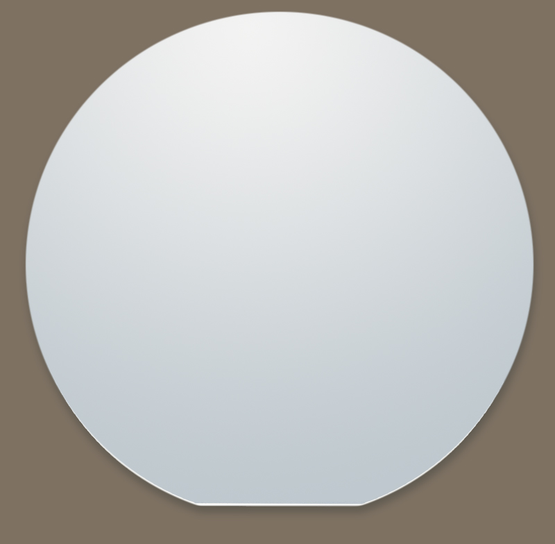
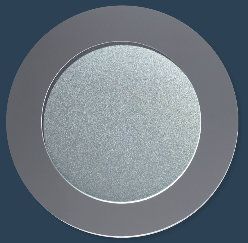
Carrier wafers and tools
–
–
Customized handling solutions for wafer and panel processing – including carriers, adapters, and chucks, tailored to your production processes.
PLANOPTIK supplies the largest semiconductor manufacturers with carrier wafers that are individually adapted to the customer’s manufacturing processes and machines.
–
–
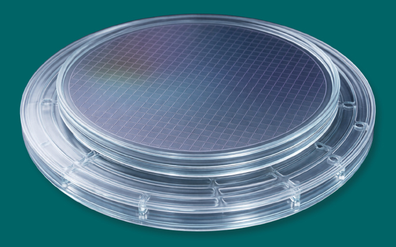
Carriers for the processing of
ultra-thin wafers
–
–
The processing of ultra-thin wafers made from brittle materials such as silicon, silicon carbide (SiC), gallium arsenide (GaAs), and other advanced semiconductor materials requires temporary mechanical support. For this purpose, the wafers are bonded to PLANOPTIK carrier wafers during processing and debonded after completion.
–
–
Carrier laser release
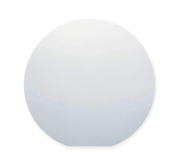
For laser release processes, PLANOPTIK provides highly transparent carrier wafers that transmit the relevant laser wavelength.
- blank carrier wafer
- easy laser release due to high transparency
- borosilicate or alkaline free glass
–
–
Carrier thermal release
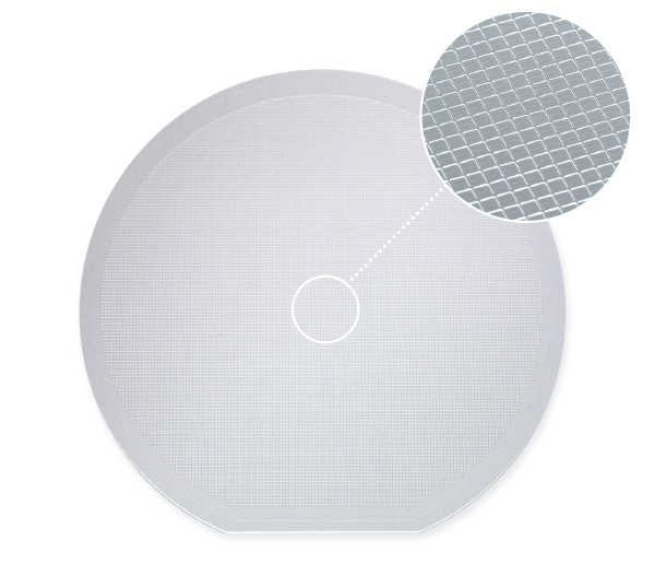
For carrier wafers that are released again by heat after bonding, PLANOPTIK offers wafers with special surface structures.
- patterned carrier wafer
- honeycomb pattern for homogenous adhesive distribution and lower ttv
- borosilicate or alkaline free glass wafers
–
–
Carrier chemical release
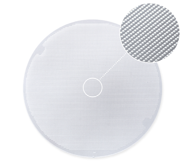
PLANOPTIK provides carrier wafers, which are to be chemically dissolved after the silicon wafers have been manufactured and processed, with up to 100,000 micro holes with a diameter of 100 µm through which the solvent reaches the wafer’s bonding layer.
- perforated carrier wafer
- high density through holes available
- fast chemical debonding
- borosilicate or alkaline free glass
–
–
Customized or off the shelf
–
–
- blank or patterned carrier wafers
- custom diameters available
- compatible with all common thin wafer handling systems
- usable with temporary bonding and debonding
- cte adapted to semiconductor device wafer
- low thickness tolerance and total thickness variation
- re-usable
- low damage laser marking for long life
- Adapter to enable handling of smaller dimensions wafers in existing equipment
- high thermal and chemical stability
–
–
How do thin-wafer-handling carriers work?
The device wafer is temporarily bonded to the carrier. As a result, the device wafer can be processed with conventional semiconductor processing systems without running the risk of being damaged due to its small thickness in the process.
–
–
What materials and sizes are available?
Thin-wafer-handling carriers can be made from various materials. The carrier material is adapted to the thermal expansion (cte) of the device wafer. This includes carrier materials adapted to Silicon, GaAs, SiC and many others. Carriers are available up to a diameter of 300mm. There are different carrier types for all commercially available debonding systems (e.g. chemical debonding, laser debonding, thermal debonding and mechanical debonding).
–
–
What are the benefits of using thin-wafer-handling carriers?
PLANOPTIK’s thin-wafer-handling carriers are characterized by their large number of variants and, in particular, by their stability and thus high reuse rate (typically more than 50 times). Thanks to many years of expertise in the field of such carriers, PLANOPTIK is able to offer solutions that are specifically tailored to customer needs.
–
–
Adapter carriers
–
–
Adapter carrier wafers are used when smaller substrates, panels or wafers need to be processed in machines that are actually designed for large wafers. The carrier wafers then have a larger diameter than the substrates, panels or wafers to be processed.
–
–
Applications of adapter carriers
Wafer-level handling
Protect thin or fragile wafers during processing in automated manufacturing processes.
Chip testing and burn-in testing
Stable individual chips or entire wafers for electrical testing.
Packaging and assembly processes
Enable the integration of chips into various packages.
Compatibility between process steps
Transfer between different wafer sizes or substrates.
Mechanical adaptation
Adapter carriers enable the use of smaller wafers in standard machines.
–
–
Tools and chucks
–
–
Customized handling devices for the processing of wafers and panels. Chucks that are individually designed and precisely tailored to your specific production processes and technical requirements.
–
–
Chucks individually adapted to your production process
Vacuum Glass Chuck
Uses vacuum to fix the wafer to the glass surface.
Electrostatic Glass Chuck (ESC)
Uses electrostatic forces to fix the wafer to the glass surface.
UV-transparent glass chuck
Specially designed for processes that require UV light transmission (e.g. UV curing or laser processes).
Temperature-controlled glass chuck
A glass chuck with integrated heating or cooling systems for regulating the temperature of the wafer.
Chemically Resistant Glass Chuck
Made from special glass materials (e.g. borosilicate glass, quartz) to resist aggressive chemicals.

–
–
Team up with PLANOPTIK
–
–

–
–
Individually developed
Are you developing a new microsystem? Are you combining microelectronics, micromechanics or microfluidics to create a new product? Are you developing a sensor, an electronic device, a fluidic system or something that has never existed before? Team up with PLANOPTIK.
–
–
Reliable partnership
In us you will find a partner who will work with you to develop electronic, mechanical, optical, chemical or biological microcomponents and has a firm grasp of materials such as glass, silicon and copper.
–
–
Together until production
PLANOPTIK also manufactures the jointly developed microcomponents and elements in high volumes using state-of-the-art wafer-based manufacturing processes.