–
–
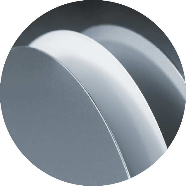
Glass wafers and panels for wafer-level packaging
–
–
PLANOPTIK supplies customized glass wafers and panels for wafer-level packaging – designed to protect, encapsulate and enable MEMS devices and photonic applications. From thin cover wafers to functional glass structures, we deliver the substrate your process needs.
Customized glass wafers and panels for wafer-level packaging-engineered for MEMS and photonics. From thin cover wafers to functional glass structures, PLANOPTIK enables reliable protection and integration at wafer level.
–
–
Customized wafers and panels
to cover your MEMS devices
by glass
–
–
Discover the technologies we offer to shape glass wafers for your WLP application. Individually developed and manufactured from R&D to high volumes.
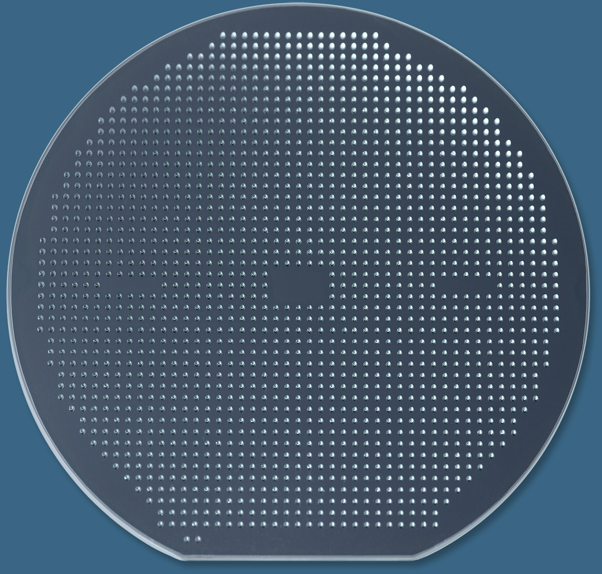
– THROUGH GLASS VIAS
– CAVITIES
– BLIND HOLES
– CHANNELS
– DIFFERENT GLASS TYPES
– MDF POLISHING
– MARKINGS
– COATINGS
– DICING
– BONDING
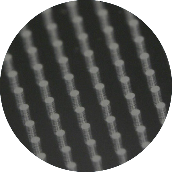
Through Glass VIAS
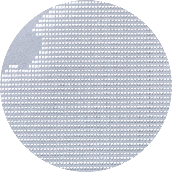
Cavities
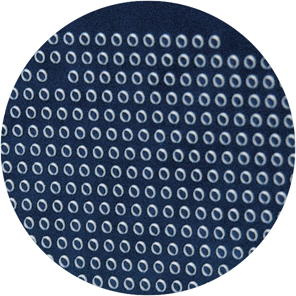
Blind holes
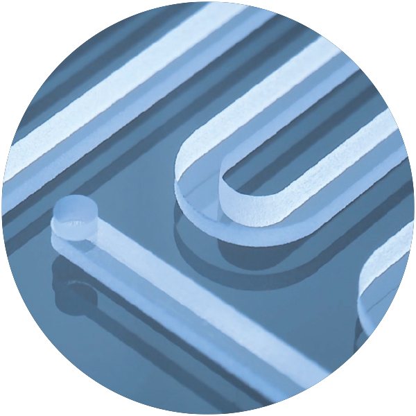
Channels
MDF Polishing
Bonding
–
–
From glass wafers to functional
sensors and MEMS devices
by wafer-level packaging
From glass wafers to functional sensors and MEMS devices by wafer-level packaging
–
–
–
–
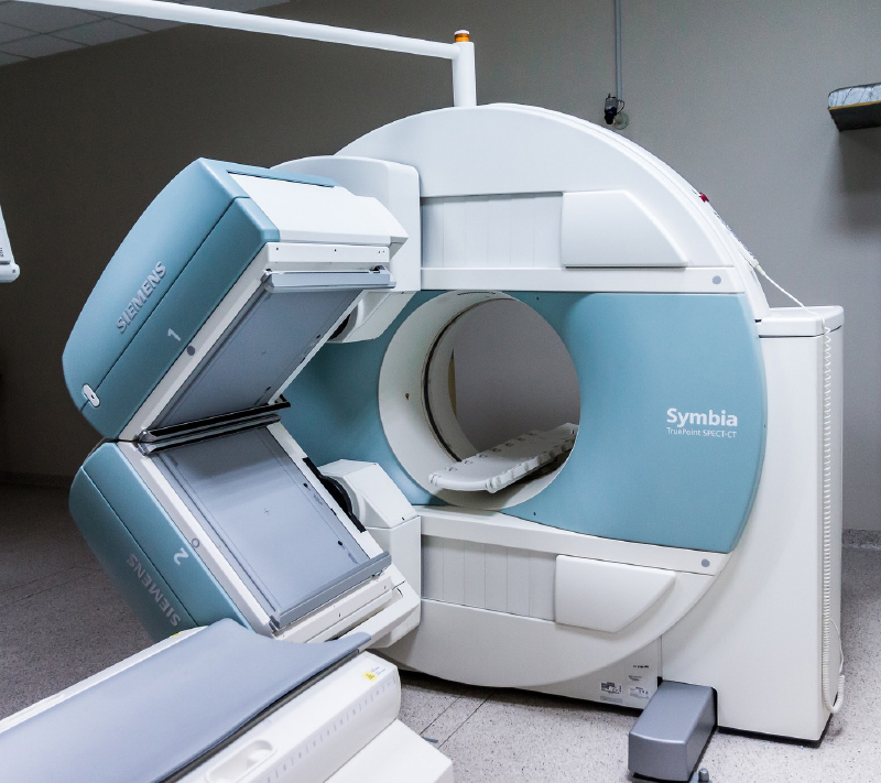
Case study: Glass wafers for covering and protecting optical sensors
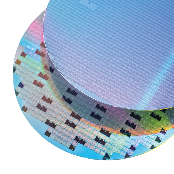
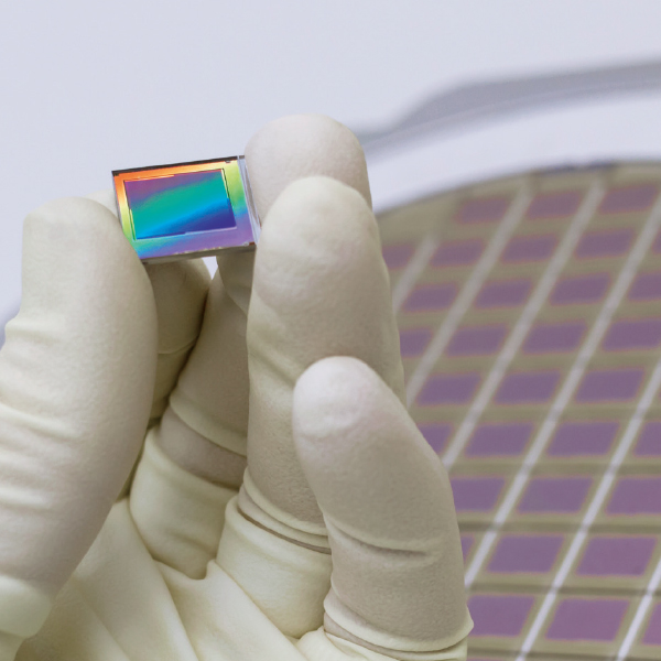
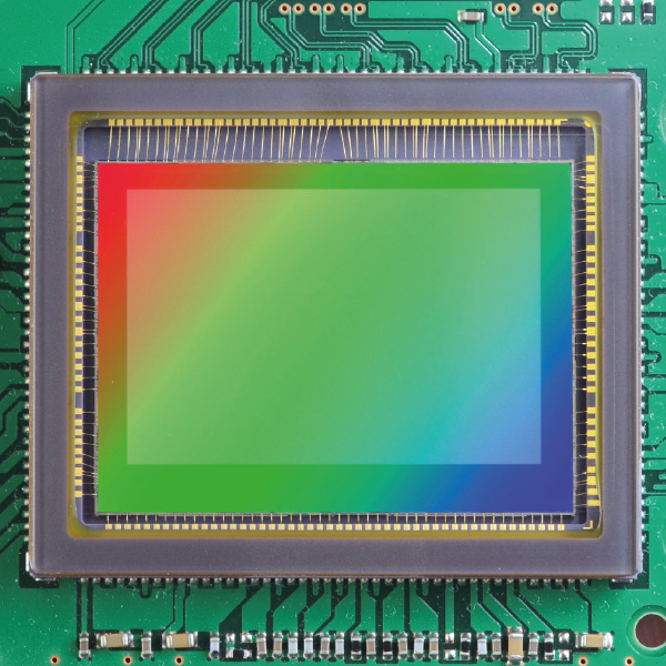
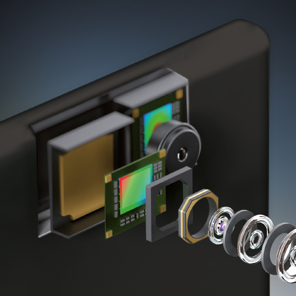
Optical sensors often require a transparent, mechanically stable and contamination-resistant cover at wafer level. PLANOPTIK provides customized glass cap wafers – either as blank glass for protection or as structured glass with cavities, channels or blind holes for added functionality.
During assembly, the glass wafer is aligned and bonded to the sensor wafer, forming a robust glass–silicon stack. After bonding, the stack is diced into individual dies, automatically encapsulating and protecting each sensor with its glass cap.
These optical sensor modules are used in industrial inspection and automation, medical imaging, consumer electronics, and automotive camera systems – where clean optics and long-term stability are critical.
–
–
Application examples for electromechanical sensors
–
–


–
–
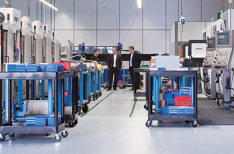
Team up with PLANOPTIK
–
–

–
–
Individually developed
Are you developing a new microsystem? Are you combining microelectronics, micromechanics or microfluidics to create a new product? Are you developing a sensor, an electronic device, a fluidic system or something that has never existed before? Team up with PLANOPTIK.
–
–
Reliable partnership
In us you will find a partner who will work with you to develop electronic, mechanical, optical, chemical or biological microcomponents and has a firm grasp of materials such as glass, silicon and copper.
–
–
Together until production
PLANOPTIK also manufactures the jointly developed microcomponents and elements in high volumes using state-of-the-art wafer-based manufacturing processes.