As technology is rapidly moving forward the reduction of device and chip size is playing an important role to be able to implement as many chips and sensors in smallest space. For this reason thickness reduction of the semiconductor wafers is necessary. Thin semiconductor wafers (thickness around 50-100 µm) are flexible and fragile. A temporary mechanical stabilization is needed in order to enable processing of the wafer and further decrease device wafer thickness.
For that the device wafers are temporarily bonded to the carrier. During processing the carrier wafer is used as a mechanical and handling support and can be detached after processing, whereby different de-bonding technologies are used:
Carriers for chemical release
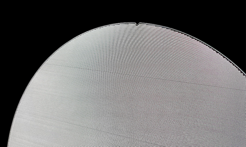
Using chemical release process, a solvent gets in contact to the adhesive and releases it. For this type of de-bonding, thousands of through holes through the carrier wafer are enabling consistent contact and fast decomposition of the adhesive.
Carrier for laser release
After processing the adhesive interlayer will be exposed by using a laser. After exposure the interlayer will lose its adhesion and the device and carrier wafers can be separated.
Carriers for thermal release
By heating up the processed wafer stack the adhesive interlayer will loose its adhesion and the device wafer can be released from the carrier by a so called shear or slide-off de-bond.
Plan Optik is offering the plain carrier (excluding the adhesives) but is closely co-operating with adhesive and equipment makers. Glass is used as carrier wafer material due to its mechanical stability and chemical resistance. All Plan Optik carrier wafers can be reused up to 30 times (depending on the details of the used process).
In order to reduce the risk of bow or warp the cte-match between semiconductor device wafer from e.g. Si, GaAs, InP or SiC can be adjusted by using different types of glass. The transparency of glass is not only used for laser de-bonding process but furthermore for in-process inspection. Also laser markings or QR-codes can be implemented for process traceability.
If you are interested to learn more about Carriers for temporary bonding and de-bonding and how these carriers can be applied to your thin wafer handling process make sure to contact us!

